

India Just Committed ₹1.28 Lakh Crore to Chips — Semicon 2.0 Is the Biggest Industrial Policy Bet in the Country's History

From Zero Fabs to a Full Ecosystem in One Cabinet Decision
On July 15, 2026, the Union Cabinet approved something that would have seemed implausible a decade ago: a ₹1.28 lakh crore outlay to build a comprehensive domestic semiconductor ecosystem from the ground up.
The India semiconductor Mission 2.0 — Semicon 2.0 — is not an incremental extension of the original ₹76,000 crore India Semiconductor Mission launched in 2021. It is a fundamental expansion in ambition, capital, and scope. While ISM 1.0 focused primarily on attracting fabrication plants and assembly and packaging units, Semicon 2.0 covers the entire semiconductor value chain: design, equipment, raw materials, fabrication, packaging, research, and talent development — simultaneously and at a scale that few countries have attempted in a single policy intervention.
For a country that currently imports over 90% of its semiconductor requirements and has, until very recently, not manufactured a single commercial chip on its own soil, this is the most consequential industrial policy announcement since the original liberalisation of 1991.
What Semicon 2.0 Actually Covers — The Six Pillars
The scheme is built around six distinct focus areas, each addressing a specific link in the semiconductor value chain that India currently lacks or needs to strengthen.
Pillar 1: Chip Design
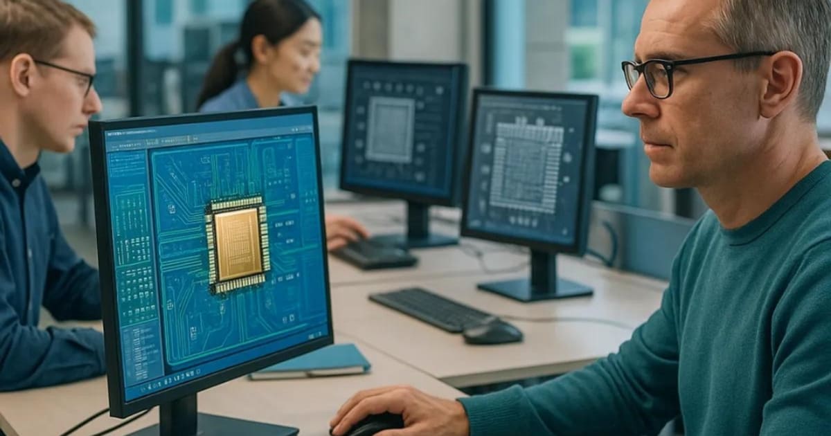
The government plans to expand support for India's chip design ecosystem. The Centre said 105 startups are already developing chips, and the new policy will back the development of semiconductor intellectual property, chip designs, and system-level products.
India's chip design capability is, by global standards, genuinely impressive. Indian engineers have contributed to the design of some of the world's most advanced processors — from Apple's A-series chips to Qualcomm's Snapdragon platform. That design competency exists at world-class level inside the R&D labs of multinationals. Semicon 2.0's design pillar is designed to catalyse a parallel layer of Indian-owned IP — startups and companies that design chips they own, not just engineers who contribute to chips owned by American companies.
Pillar 2: Semiconductor Equipment and Materials
The scheme will extend incentives to companies manufacturing semiconductor equipment, chemicals, gases, and materials required for chip production. The government said this is aimed at creating a domestic supply chain for semiconductor manufacturing.
This is the pillar that most policymakers in other countries underestimate. A fabrication plant is only as independent as its supply chain allows it to be. If every chemical, every process gas, every piece of lithography equipment must be imported — primarily from the US, Europe, and Japan — then the "Made in India" chip is only partially made in India. Semicon 2.0's commitment to building an equipment and materials ecosystem alongside the fabs themselves reflects a more sophisticated understanding of semiconductor sovereignty than the original ISM design.
Pillar 3: Fabrication Plants
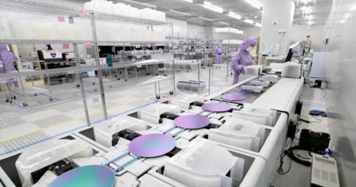
On the manufacturing front, Semicon 2.0 is eyeing to attract more chipmakers to set up facilities in India, including silicon fabs, compound semiconductor fabs, discrete component fabs and display fabs.
The country's first semiconductor fab is expected to be commissioned in 2028. The Tata Electronics facility at Dholera in Gujarat — partnered with Taiwan's Powerchip Semiconductor Manufacturing Corporation — targeting 28nm and below process nodes, is the primary near-term milestone under this pillar.
Pillar 4: ATMP and OSAT
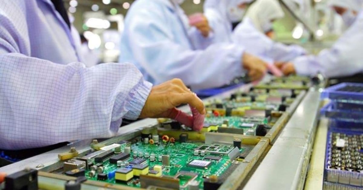
The policy will continue support for Assembly, Testing, Marking and Packaging facilities and Outsourced Semiconductor Assembly and Test units, with the government aiming to attract more advanced packaging technologies to India.
The Micron facility in Sanand — inaugurated by PM Modi in February 2026 — represents the most tangible proof of concept in this category.
Micron's $825 million ATMP facility, processing DRAM and NAND flash memory for mobile, data centre, and automotive applications, has validated that India can deliver the power, water, workforce, and regulatory environment that a global semiconductor company requires.
Pillar 5: Research and Development
Semicon 2.0 significantly expands India's semiconductor R&D commitment — covering materials science, process technology, device physics, and next-generation packaging architectures. The goal is not just to manufacture existing chip designs, but to develop the fundamental research capability required to remain competitive as semiconductor technology evolves.
Pillar 6: Talent Development
The final pillar addresses the most fundamental constraint on India's semiconductor ambitions: the availability of engineers who understand semiconductor manufacturing rather than just semiconductor design. Running a fab requires process engineers, materials scientists, equipment specialists, and yield management experts — a profile that India's engineering education system has not historically produced at scale. Semicon 2.0 commits to building that pipeline through a combination of curriculum reform, specialised programmes, and partnerships with global semiconductor companies.
Why ISM 1.0 Needed a Much Bigger Successor
The India Semiconductor Mission was launched in December 2021 with an outlay of ₹76,000 crore — at the time, a genuinely significant commitment that placed India in the same league as several established Asian semiconductor hubs in terms of government support per project.
ISM 1.0 approved fourteen projects and attracted meaningful investment from Micron, Tata Electronics (partnered with Powerchip), CG Power (partnered with Renesas and Stars Microelectronics), and others. The total investment committed under ISM 1.0, across all approved projects, exceeded ₹1.60 lakh crore from the private sector — a significant multiplier on the government's incentive outlay.
But ISM 1.0 had a specific and important limitation: it focused on the plants, not the ecosystem around the plants. A fab that imports all its process chemicals, all its specialty gases, all its lithography equipment, and all its wafers is operationally sovereign but supply-chain dependent. A domestic semiconductor industry that is entirely reliant on foreign equipment and materials cannot truly be called self-reliant.
Semicon 2.0 expands beyond the plants to include the chemicals, gases, equipment, and materials that feed those plants — a fundamentally more ambitious vision of what semiconductor self-reliance means. And it adds R&D and talent as explicit pillars rather than afterthoughts, recognising that the knowledge base required to sustain a semiconductor industry cannot simply be imported alongside the machinery.
The doubling of the outlay from ₹76,000 crore to ₹1.28 lakh crore reflects the government's assessment that achieving genuine ecosystem depth — rather than just individual plant investments — requires meaningfully more capital at the policy support level.
Why July 2026 Is the Right Moment for This Announcement
The timing of the Semicon 2.0 approval is not accidental. It comes at the moment when India's semiconductor journey has produced its first tangible results, the global policy environment for supply chain diversification is at its most urgent, and the case for doubling down has been validated by early evidence.
Micron's Sanand facility began commercial operations in early 2026 — the first semiconductor facility of the current mission cycle to go live. The Tata-Powerchip fab at Dholera has received its construction approvals and is targeting first silicon by late 2026. Qualcomm completed a 2nm chip tape-out with design work done entirely across its Indian engineering centres. The foundation stone for the HCL-Foxconn semiconductor unit in Uttar Pradesh was laid with PM Modi in attendance.
These are not paper commitments. They are physical milestones — buildings being built, equipment being installed, engineers being hired. Semicon 2.0 arrives as the successor policy at exactly the right moment: when ISM 1.0 has proven the concept but the ecosystem remains too nascent to be self-sustaining without continued government support.
The global context adds urgency. The US CHIPS Act committed $52 billion to domestic semiconductor manufacturing. The EU Chips Act committed €43 billion. South Korea committed $23 billion. China's semiconductor support programme has exceeded $94 billion. India at ₹1.28 lakh crore — approximately $15 billion at current exchange rates — is moving into a comparable range with serious mid-tier semiconductor nations, while remaining well below the US and China in absolute terms.
For geopolitical context: as US export controls on advanced chips tighten, as China's semiconductor ambitions accelerate, and as the global technology industry seeks to diversify its chip supply chains away from concentration in Taiwan, India's credibility as an alternative semiconductor geography improves with every milestone delivered.
The Design Ecosystem — India's Hidden Strength Gets Policy Support
The most underappreciated dimension of India's semiconductor story is that the design capability already exists, at genuinely world-class level, and has been operating at that level for three decades.
Multinational companies have conducted semiconductor research and development in India since the 1990s. Intel, Qualcomm, Broadcom, Nvidia, AMD, Texas Instruments, and dozens of other global chip companies operate significant engineering centres in India. The engineers working in those centres have contributed to some of the most advanced semiconductor designs in human history.
What has not existed — until ISM 1.0 and now Semicon 2.0 — is a policy framework to support Indian-owned chip design companies building their own IP. Under the Design-Linked Incentive scheme enhanced under Semicon 2.0, companies get access to Electronic Design Automation tools, IP cores, and financial support for chip tape-outs — the expensive process of translating a chip design into a physical prototype.
The 105 startups already developing chips, cited in the Cabinet statement, represent the seed of what could become a genuinely significant Indian fabless semiconductor industry — companies that design chips but outsource fabrication, in the model pioneered by Qualcomm, Nvidia, and Apple. If Semicon 2.0's design pillar successfully scales this to 300–500 active design companies over its policy horizon, India will have built the intellectual property layer of its semiconductor industry — the highest-margin, most strategically valuable part — alongside the manufacturing layer being built through the fab investments.
The 2028 Milestone — When India Gets Its First Commercial Fab
The single most consequential date in Semicon 2.0's timeline is 2028: the expected commissioning of India's first commercial semiconductor fabrication plant.
The Tata Electronics facility at Dholera, Gujarat — partnered with Taiwan's Powerchip Semiconductor Manufacturing Corporation — is the facility most likely to deliver on that 2028 timeline. The fab is designed to produce chips at 28nm and below process nodes, covering automotive chips, industrial microcontrollers, display drivers, and IoT devices — the mature-to-advanced range that covers the majority of chips India currently imports.
Twenty-eight nanometre technology is not cutting-edge by global standards — TSMC is manufacturing at 2nm, and 3nm chips are now in mass production. But it is the process node that covers the majority of chips used in India's fastest-growing end markets: automotive electronics, industrial automation, consumer electronics, and the power management chips that go into every EV battery system. India does not need to manufacture 2nm AI training chips to achieve meaningful semiconductor self-sufficiency. It needs to manufacture the chips that go into everything it actually builds.
If the Dholera fab commissions on schedule in 2028 and achieves commercial scale by 2029, India will have crossed a threshold that no other large economy had crossed before it entered the semiconductor mission: actually producing chips for domestic consumption in meaningful quantities. That milestone — first silicon from a domestic fab — is when the semiconductor story stops being a policy announcement and becomes an industrial reality.
Challenges That Semicon 2.0 Must Address
No honest assessment of India's semiconductor ambitions can omit the persistent structural challenges that have slowed progress and must be addressed for Semicon 2.0 to deliver on its promise.
Power and Water at Scale.
Each semiconductor fab requires 24x7 uninterrupted power — something India's grid has historically been unable to guarantee uniformly — and over 10 million litres of ultra-pure water per day for the most advanced processes. Addressing these infrastructure requirements at the specific locations where fabs are being built is a necessary condition for on-schedule commissioning.
Regulatory Speed.
India's single-window clearance systems have improved significantly but regulatory approval timelines for large industrial projects remain longer than in competing semiconductor geographies. South Korea, Taiwan, and the UAE have all demonstrated faster regulatory throughput for semiconductor investment — a disadvantage India needs to narrow.
Equipment Import Dependency.
Even with Semicon 2.0's new focus on domestic equipment and materials, building a meaningful domestic supplier base for the most specialised semiconductor equipment — lithography systems, ion implanters, chemical mechanical planarisation tools — will take years. In the interim, India's fabs will remain dependent on equipment from ASML, Applied Materials, Lam Research, and Tokyo Electron.
Trained Workforce at Scale.
The talent pillar of Semicon 2.0 is perhaps the most time-constrained. Training semiconductor process engineers takes three to five years after undergraduate education. Building the curriculum, the faculty, and the laboratory infrastructure to produce thousands of such engineers annually is a multi-year programme that needs to have started yesterday.
These challenges are real and must be acknowledged. But they are also the challenges that every successful semiconductor nation has faced and addressed through sustained policy commitment, institutional capacity building, and the patient deployment of capital over ten to fifteen year horizons. Taiwan, South Korea, and the United States all navigated versions of the same structural challenges on their own semiconductor journeys.
The Beneficiaries — Who Gains From Semicon 2.0
The approval of Semicon 2.0 has immediate and medium-term implications for specific categories of companies.
Indian conglomerates with semiconductor investments — Tata Electronics, HCL (through its Foxconn JV), CG Power, and Kaynes Technology — gain policy certainty and potentially enhanced incentive structures for their existing committed projects. Semicon 2.0's approval confirms that the government's semiconductor commitment extends beyond the initial ISM 1.0 framework and will be maintained through the decade required to deliver results.
Semiconductor equipment and materials companies — currently a thin category in India but the segment that Semicon 2.0 most explicitly tries to grow — stand to benefit from both incentive support and the creation of a domestic customer base as Indian fabs come online. Companies that can supply specialty chemicals, process gases, or semiconductor test equipment to Indian facilities will have a market that simply did not exist three years ago.
Global semiconductor companies considering India as a manufacturing or R&D location gain a clear signal of policy continuity. A ₹1.28 lakh crore commitment is not something a government walks back easily. The policy horizon that Semicon 2.0 establishes — extending the mission at doubled capital and expanded scope — makes India a more credible 10–15 year investment destination for companies considering manufacturing expansions.
Design startups and fabless chip companies — the 105 already developing chips cited in the Cabinet statement — gain access to enhanced EDA tools, IP cores, and DLI scheme benefits that make chip tape-outs economically viable for early-stage companies that previously couldn't absorb those costs.
The Bigger Picture — What India Is Actually Building
Step back from the specific components of Semicon 2.0 and the strategic ambition becomes clear. India is building — for the first time in its independent history — a domestic capability to design, manufacture, package, test, and eventually export semiconductor chips. Not on every process node, not for every application, not in competition with Taiwan's most advanced production. But in the specific applications, at the specific process nodes, and with the specific supply chain depth that reduces the critical dependencies that have made India's technology sector structurally vulnerable.
The dependence on imported chips is not just an economic issue. In a world where semiconductors have become geopolitically contested — where the US restricts chip exports to China, where Taiwan's security situation creates supply chain anxiety for every electronics manufacturer, where AI capabilities are increasingly viewed as national security assets — India's 90% import dependence is a strategic vulnerability of the first order.
Semicon 2.0 is the government's most serious attempt to address that vulnerability at scale. The ₹1.28 lakh crore outlay, spread across six pillars and multiple years, will not eliminate import dependence overnight. But it creates the conditions under which, by 2030 or 2032, India could manufacture domestically the chips required for a significant share of its automotive, consumer electronics, industrial, defence, and AI infrastructure applications.
That is the prize. And ₹1.28 lakh crore — alongside the private sector investment it is designed to catalyse — is the price of being in the game.

Nikunjj Jhawar is a Chartered Accountant (CA) and Chartered Financial Analyst (CFA) with nearly two decades of experience in the financial services industry. Having worked with global institutions such as HSBC and Credit Suisse in investment-related roles, he brings deep expertise in finance and markets. He is the Founder of mangopeoplenews.com, where he focuses on making complex topics in finance, markets and business accessible and relevant to everyday readers.
